


 Open WeChat, scan

JSSI For Bumping
Equipment in each process is leading brand in the industry ENG/MFG in JSSI own high debugging and mass production experience

JSSI For Traditional Package

JSSI Turn-key Technical Solution
Design Service Package Service Test Service

JSSI For BGA
JSSI For BGA
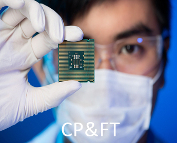
JSSI Product Test Capability——CP&FT
JSSI Product Test Capability——CP&FT

JSSI For WLCSP
JSSI Core Equipment for Traditional PackageJSSI Core Equipment for Traditional PackageJSSI Core Equipment for Traditional Package
2020
The company was formally established on Sep 11th 2020
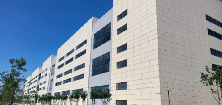
54000
54000 square meters standardized fab environment
1
“One Hour” To Nanjing Lukou International Airport
“One Hour”To Shanghai
“Three Hour”To Beijing


 Open WeChat, scan
 苏公网安备 32011102010379号 | 苏ICP备2021018400号-1